Your Thin Films Visualized
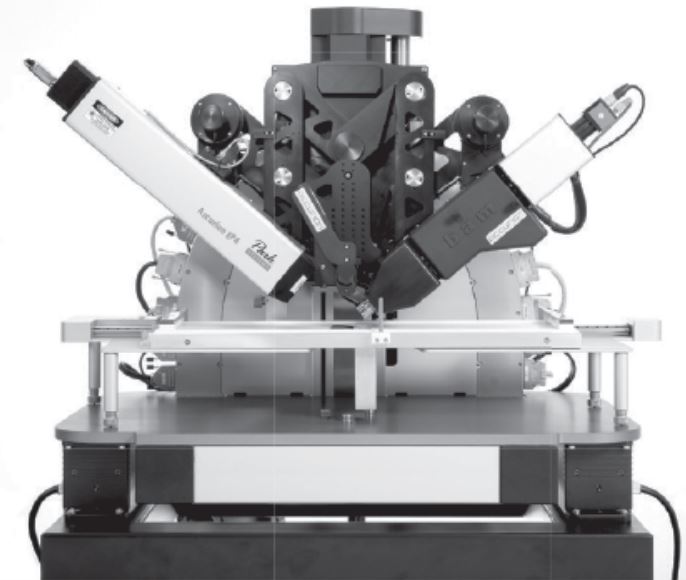
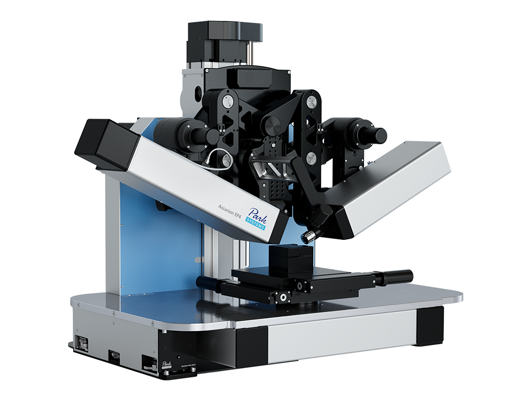
The Accurion EP4 offers a variety of unique features that allow the visualization of your surface in real-time. You will see in real-time the structure of your sample on a microscopic scale. You can measure parameters like thickness, refractive index, and absorption. You can receive maps of selected areas. You can combine the instrument with other technologies like AFM, QCM-D, reflectometry, Raman spectroscopy and many more to receive even more information from your samples. The Accurion EP4 is a modular instrument enabling configuration for your specific measurement tasks. The Accurion EP4, equipped with the standard laser can also be operated as a Brewster angle microscope, typically in LB applications.
-
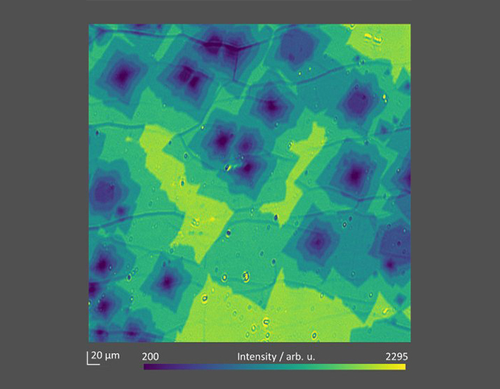
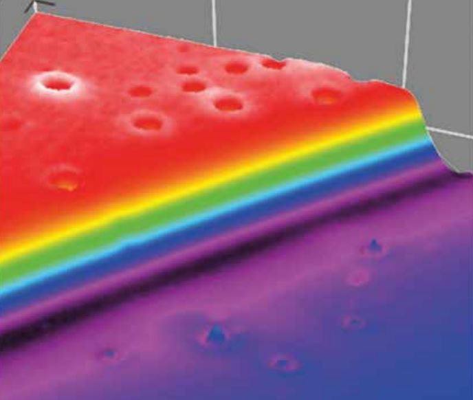
01 Graphene, 2D-materials
Imaging ellipsometry allows the direct visualization of your 2D-material flakes on various substrates/materials. It is possible to measure thickness and optical properties of different 2D-material layers in the micrometer scale.
-
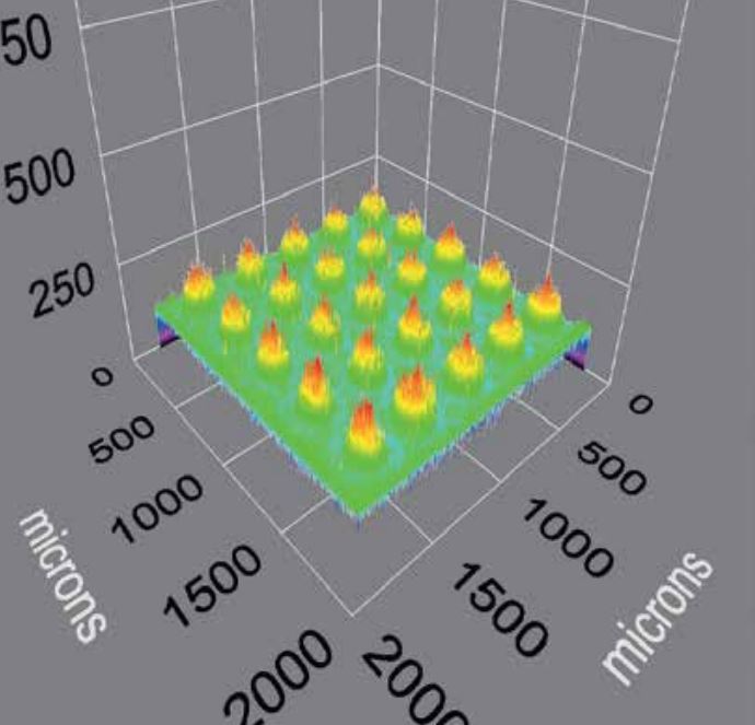
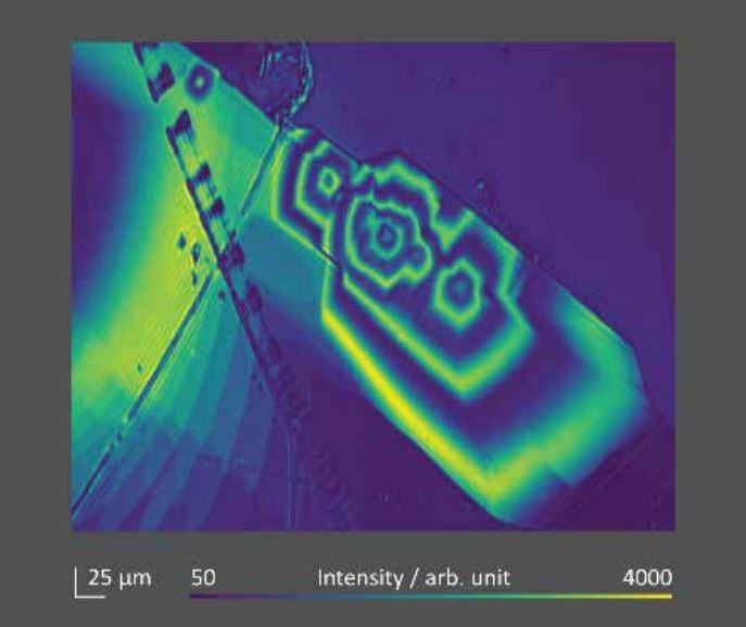
02 Photonics, Displays, MEMs
Imaging ellipsometry allows the direct visualization of your 2D-material flakes on various substrates/materials. It is possible to measure thickness and optical properties of different 2D-material layers in the micrometer scale.
-
03 Surface engineering
The main attempt of silanization is to form bonds across the interface between mineral/inorganic components and organic components present in paints, adhesives, etc., or as the anchor for further steps of surface modifications.
-
04 Air/Water or Liquid/Liquid Interface
The air/water interface is of elementary interest in biophysics as well as in industrial applications. Brewster angle/LIQUID microscopy (BAM) is a powerful technique that allows for real-time visualization of Langmuir-Blodgett monolayers.
-
05 Bio Interfaces
Biological applications demand high sensitivity observation techniques. Additionally, the environment needs to be controllable in order to avoid influencing or damaging the behavior of observed materials. Imaging Ellipsometry offers highest sensitivity for thickness or surface coverage of mono- as well as sub-monolayers with microscopic resolution.
-
06 Organic electronics, solar cells
Considering that the optimal parameters play a central role in understanding and tailoring the properties of thin conductive polymers and that microscopic applications such as solar cells or OLEDs are increasingly coming to the fore, imaging ellipsometry is the method of choice to determine these parameters.
-
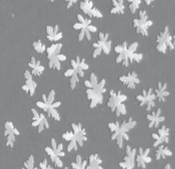
07 Anisotropic films
Anisotropic micro crystals show high potential for the applications in e.g. microelectronic devices and flexible electronics. Most organic single crystals indicate a highly anisotropic optical behavior. Regarding anisotropic samples, the refractive index depends on the polarization of light and direction of propagation.
-
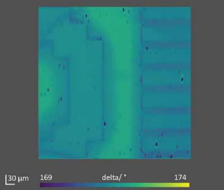
08 Various other applications
A wide selection of samples with structures can be visualized and measured with the unique technique of imaging ellipsometry. If you do not find your application in this overview, feel free to contact us for specific information.