Surface Inspection Metrology of Nanofilms
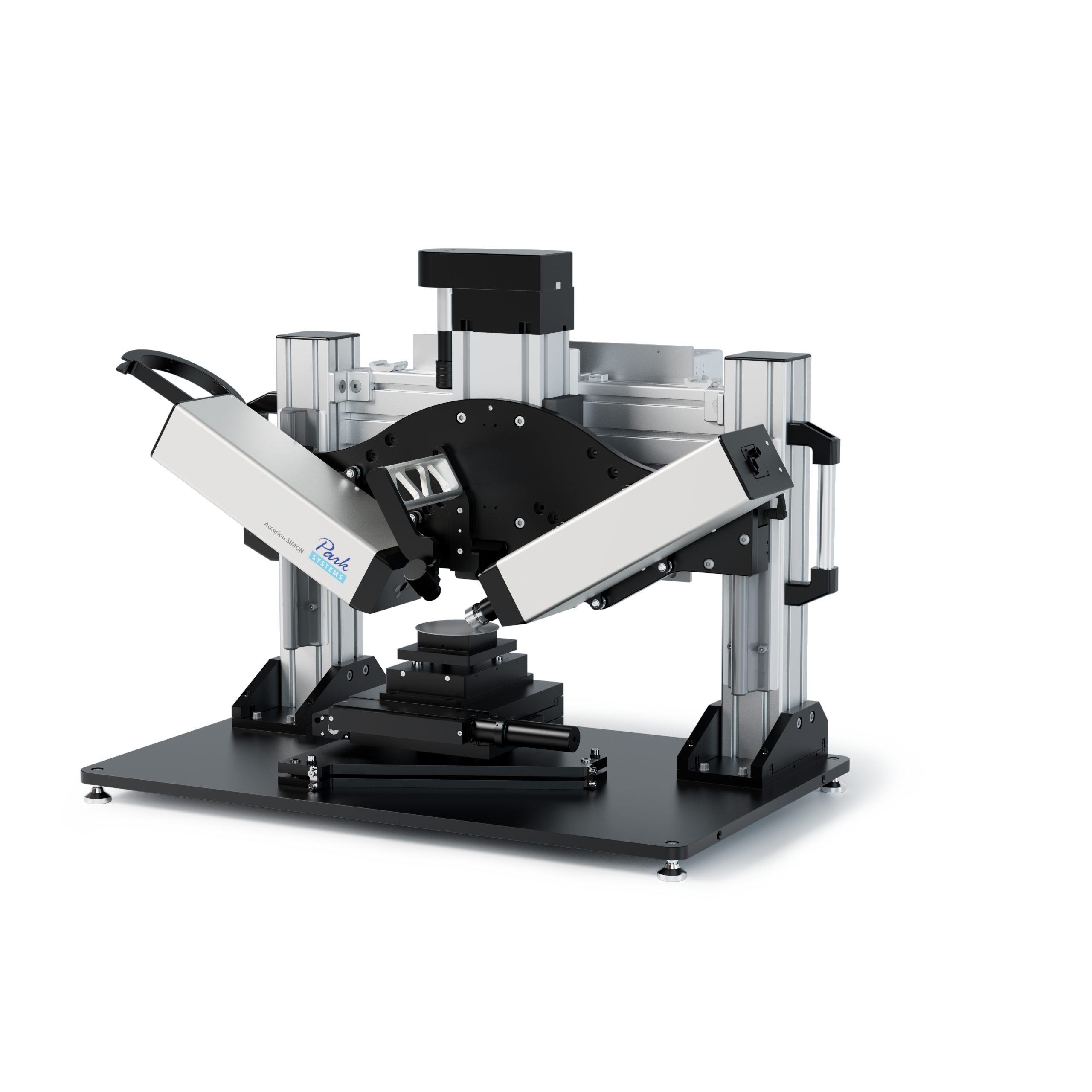
SIMON is specifically designed for routine measurement tasks. Its simple user interface and robustness of a fixed angle ellipsometer enables the entry to imaging ellipsometry. It can be operated in two different modes. The microscopic mode is very fast and allows to visualize variations and defects in thinnest layers (e.g. monolayers: d = 0.35 nm), whereas the ellipsometric mode measures thickness and the refractive index of the sample materials. Imaging Ellipsometry itself combines the sensitivity of thickness and refractive index measurements with the imaging of microscopy. This allows determining thickness and refractive index variations with microscopic images on e.g. micro-structured samples. Typical applications include the surface inspection of homogeneities and defects of large samples in quality control or the fast localization of flakes of 2D Materials.
-
Typical Applications
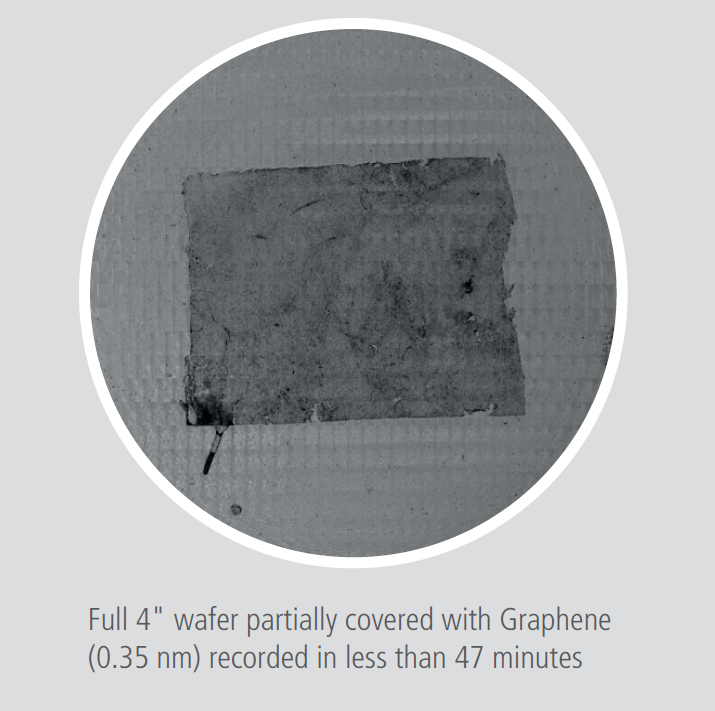
Large Area Inspection and Automatic Flakesearch SIMON is designed to automatically stitch large areas with smooth transitions. A complete 4” wafer can be inspected within 47 minutes, whilst observing defects, particles and inhomogoneities as small as 10 μm. SIMON also allows searching for flakes or materials with desired thicknesses. Through the imaging aspect of SIMON, histogram analysis on a single measurement becomes possible and provides a detailed insight into the distribution of thicknesses or inhomogeneities.
-
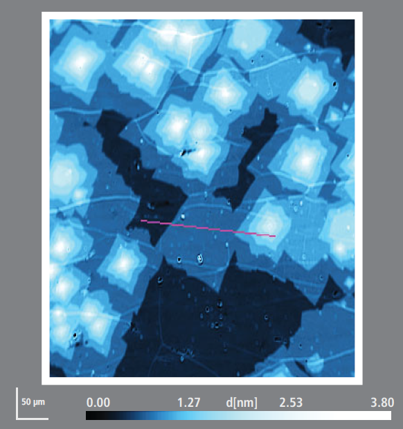
Thickness Mapping
The combination of ellipsometry and microscopy allows to measure the thickness maps of your sample. These maps are comparable to AFM measurements, but can also be measured for non top layers. Additionally, imaging ellipsometry will measure the thickness map of approx.500 μm (X) x 550 μm (Y) in less than 1 minute. The thickness resolution is below 0.01 nm within a range of 0.01 nm < d < 5 μm*. The ellipsometric mode also determines the refractive index. This allows users to determine refractive index variation, that e.g. occurs in holographic gratings scribed by a laser. Small changes in refractive index, as for example seen in waveguides, can thus be visualized and observed. *Depending on sample/substrate combination